Professional industry ceramic supplier, silicon nitride, silicon carbide, aluminum nitride and any other kinds of ceramics.
1. Introduction
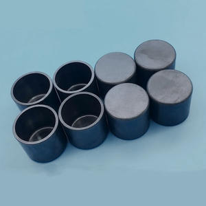
Just 24 hours ago, Wolfspeed announced a major expansion of its silicon carbide wafer production facility in Germany—part of a global race to meet surging demand for power electronics in electric vehicles and renewable energy systems. At the heart of this manufacturing leap lies a surprisingly unsung hero: the silicon carbide crucible. While headlines focus on chips and EVs, it’s these ultra-durable, thermally stable containers that enable the precise, high-purity crystal growth needed for next-generation semiconductors.

In niche industrial applications where temperatures exceed 1,600°C and even trace impurities can ruin a multi-million-dollar batch, material choice isn’t just important—it’s make-or-break. That’s where the silicon carbide crucible shines, quite literally, under extreme conditions.
2. Why Silicon Carbide Crucibles Dominate Advanced Crystal Growth
Growing single-crystal silicon carbide or gallium nitride requires molten precursors held at temperatures often above 2,000°C in inert or controlled atmospheres. Standard ceramic crucibles made from alumina (Al2O3) or zirconia (ZrO2) simply can’t withstand this without reacting, degrading, or leaching contaminants.
Silicon carbide crucibles offer three game-changing advantages:
- Exceptional thermal conductivity (up to 120 W/m·K), enabling uniform heat distribution and reducing thermal stress cracks in growing crystals.
- Outstanding chemical inertness—resisting attack from molten Si, Ga, and nitrogen-rich vapors that corrode other ceramics.
- Minimal thermal expansion mismatch with the growing SiC crystal, lowering dislocation density and improving wafer yield.
These properties make silicon carbide crucibles indispensable in physical vapor transport (PVT) and sublimation-based crystal growth methods—the industry standard for bulk SiC ingots.
3. Silicon Carbide vs. Alternatives: Boron Carbide, Alumina, and Silicon Nitride
When engineers evaluate containment solutions for ultra-high-temperature processes, they often compare silicon carbide to other advanced ceramics. Let’s clarify the distinctions.
3.1 Boron Carbide vs Silicon Carbide
Boron carbide (B4C) is harder and lighter than silicon carbide, making it ideal for armor and abrasives. However, it oxidizes rapidly above 500°C in air and reacts with many molten metals. In contrast, silicon carbide forms a protective silica layer that enhances stability up to 1,600°C in oxidizing environments—and performs even better in inert atmospheres used in crystal growth. For crucible applications, silicon carbide wins on thermal stability and compatibility.
3.2 Alumina and Zirconia Crucibles
Alumina (Al2O3) and zirconia crucibles are common in labs and lower-temperature metallurgy. But both suffer from reactivity with silicon and gallium compounds. Alumina can introduce oxygen impurities; zirconia may destabilize under thermal cycling. Neither matches silicon carbide’s combination of purity, strength, and thermal shock resistance at extreme temperatures.
3.3 Silicon Nitride: A Different Role Altogether
Silicon nitride (Si3N4) is another advanced ceramic prized for its fracture toughness and thermal shock resistance—but it’s rarely used as a crucible for molten semiconductor materials. Instead, you’ll find silicon nitride rings, plates, and custom heat shields in furnace support structures. While a silicon nitride crucible factory might serve niche R&D needs, silicon carbide remains the go-to for actual melt containment due to its superior high-temperature stability in reactive environments.
4. Beyond Crucibles: The Broader Ecosystem of Silicon Carbide Components
The same material science that enables robust silicon carbide crucibles also powers a range of supporting components in semiconductor and high-temp industrial systems:
- Silicon carbide burner nozzles and tubes handle aggressive combustion gases in furnaces.
- RBSiC (reaction-bonded silicon carbide) tile blocks and ceramic columns provide structural support in kilns.
- Silicon carbide thermocouple protection tubes shield sensors in harsh environments.
- Even silicon carbide ceramic discs and grinding tools are used to finish wafers post-growth.
Interestingly, while consumer products like silicon carbide ceramic baking dishes or dinner plates exist, they’re typically made from sintered composites with lower purity—nowhere near the grade required for semiconductor crystal growth. The crucibles used in fabs are engineered for ultra-high purity, often exceeding 99.9% SiC content.
5. Future Outlook and Material Innovation
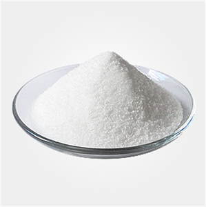
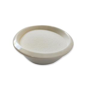
As the demand for larger-diameter, lower-defect SiC wafers grows, crucible design is evolving. Researchers are experimenting with coated silicon carbide crucibles, composite liners, and tailored porosity to further suppress impurity diffusion. Meanwhile, the high purity silicon nitride powder market is expanding to support complementary furnace hardware—but not as a direct replacement for the crucible itself.
Companies investing in vertical integration, like Wolfspeed and II-VI (now Coherent), often manufacture their own crucibles in-house to control quality. This underscores how mission-critical the silicon carbide crucible has become—not just a container, but a key enabler of the entire wide-bandgap semiconductor supply chain.
6. Conclusion
From electric vehicle inverters to 5G base stations, the performance of modern power electronics traces back to flawless crystal growth—and that starts with the right crucible. In this high-stakes arena, the silicon carbide crucible stands unmatched. While materials like boron carbide, alumina, and silicon nitride each have their place, none combine the thermal, chemical, and mechanical properties needed to reliably contain molten semiconductor precursors at extreme temperatures. As the semiconductor industry pushes toward larger, purer crystals, expect the humble silicon carbide crucible to remain at the center of innovation.
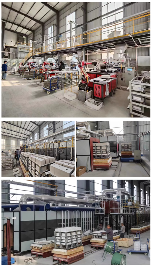
Our Website founded on October 17, 2012, is a high-tech enterprise committed to the research and development, production, processing, sales and technical services of ceramic relative materials such as Silicon. Our products includes but not limited to Boron Carbide Ceramic Products, Boron Nitride Ceramic Products, Silicon Carbide Ceramic Products, Silicon Nitride Ceramic Products, Zirconium Dioxide Ceramic Products, etc. If you are interested, please feel free to contact us.
RELATED POSTS
How to Properly Use and Maintain a Silicon Carbide Crucible: A Step-by-Step Guide
Silicon Carbide Crucibles: The Backbone of High-Temperature Industrial and Artisan Applications
What Makes Silicon Carbide Crucibles Essential in Modern High-Temperature Applications?
Silicon Carbide Crucibles Power Next-Gen Semiconductor Crystal Growth
Silicon Carbide Crucibles: High-Performance Solutions for Extreme Industrial and Laboratory Applications