Professional industry ceramic supplier, silicon nitride, silicon carbide, aluminum nitride and any other kinds of ceramics.
1. Introduction
When you think of cutting-edge tech—smartphones, electric vehicles, or satellite systems—you rarely consider the humble crucible that helped forge their core components. Yet behind every high-performance semiconductor lies a silent workhorse: the silicon carbide crucible. Unlike everyday ceramic dinnerware or decorative silicon carbide ceramic plates for dinner, this specialized vessel operates in environments exceeding 1600°C, where even minor impurities can ruin an entire batch of semiconductor material. In this article, we’ll dive into how silicon carbide crucibles enable one of the most demanding industrial processes on Earth: crystal growth for next-generation electronics.
2. Why Silicon Carbide? The Material Advantage
Silicon carbide (SiC) isn’t just another ceramic—it’s an advanced ceramic engineered for extremes. With exceptional thermal conductivity, outstanding resistance to thermal shock, and remarkable chemical inertness, silicon carbide stands apart from traditional refractories like alumina (Al2O3) or zirconia (ZrO2). While zirconia crucibles are common in lower-temperature lab settings, they degrade rapidly when exposed to molten silicon or aggressive fluxes used in crystal pulling. Similarly, boron carbide vs silicon carbide comparisons often favor SiC for crucible applications due to better oxidation resistance and manufacturability at scale.
What truly sets silicon carbide apart is its ability to maintain structural integrity while cycling repeatedly between room temperature and over 2000°C. This makes it ideal for directional solidification or Czochralski (CZ) methods used to grow single-crystal ingots. Crucibles made from reaction-bonded silicon carbide (RBSiC)—including rbsic silicon carbide tile blocks or custom-formed crucibles—offer near-zero porosity and minimal contamination, ensuring the purity required for semiconductor-grade materials.

3. Real-World Application: Growing Silicon and Compound Semiconductors
In semiconductor fabs, the silicon carbide crucible serves as the primary container for melting ultra-pure polysilicon before it’s slowly crystallized into monocrystalline ingots. These ingots are then sliced into wafers that become the foundation of integrated circuits. Any metallic impurity leaching from the crucible—iron, nickel, or even aluminum—can create electron traps that cripple device performance. Silicon carbide’s low solubility in molten silicon and minimal vapor pressure at high temperatures make it uniquely suited for this task.
Beyond elemental silicon, silicon carbide crucibles are also indispensable in growing compound semiconductors like gallium arsenide (GaAs) or indium phosphide (InP), used in high-frequency RF chips and optoelectronics. These melts are highly corrosive, quickly attacking alumina or graphite linings. Here, dense silicon carbide crucibles provide both containment and thermal stability, enabling consistent crystal quality across production runs.
4. Comparison with Other Advanced Ceramics
While silicon nitride (Si3N4) is another high-performance ceramic—used in everything from custom silicon nitride heat shields to silicon nitride crucible factories—it’s less common in direct melt contact due to potential nitrogen release and higher cost. Similarly, boron nitride ceramics offer excellent non-wetting properties but lack the mechanical strength needed for large-scale crucibles. Aluminum oxide (alumina) and zirconia crucibles, though widely available, simply can’t match silicon carbide’s combination of thermal shock resistance and chemical stability at extreme temperatures.
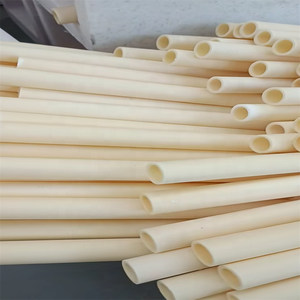
Even within the silicon carbide family, not all forms are equal. Sintered SiC offers the highest purity but is expensive; RBSiC provides a cost-effective balance of performance and scalability. Meanwhile, products like silicon carbide ceramic tubes, silicon carbide burner nozzles, or silicon carbide brick share the same base material science but are optimized for different industrial roles—from furnace linings to fluid handling.
5. Beyond the Crucible: Supporting Infrastructure
The ecosystem around silicon carbide crucibles includes complementary components like silicon carbide thermocouple protection tubes, silicon carbide ceramic columns for structural support, and even silicon carbide rings used as sealing elements in vacuum furnaces. These parts ensure the entire crystal growth system remains contamination-free and thermally efficient. Interestingly, while consumer items like silicon carbide ceramic baking dishes or silicon carbide ceramic serving bowls leverage SiC’s thermal properties for kitchen use, they’re made from food-safe, lower-density formulations—far removed from the high-purity, dense variants used in semiconductor manufacturing.
6. Conclusion
The silicon carbide crucible may be invisible to end users, but it’s foundational to the modern digital age. By enabling reliable, high-purity crystal growth under punishing conditions, it supports everything from solar cells to 5G infrastructure. As demand for wide-bandgap semiconductors like SiC itself grows, the need for even more robust and pure crucibles will only intensify—cementing silicon carbide’s role not just as a material, but as a mission-critical enabler of technological progress.
Our Website founded on October 17, 2012, is a high-tech enterprise committed to the research and development, production, processing, sales and technical services of ceramic relative materials such as Silicon. Our products includes but not limited to Boron Carbide Ceramic Products, Boron Nitride Ceramic Products, Silicon Carbide Ceramic Products, Silicon Nitride Ceramic Products, Zirconium Dioxide Ceramic Products, etc. If you are interested, please feel free to contact us.
RELATED POSTS
How to Properly Use and Maintain a Silicon Carbide Crucible: A Step-by-Step Guide
5 Key Comparisons That Define the Performance of Silicon Carbide Crucibles in Modern Industry
7 Essential Facts About Silicon Carbide Crucibles and Their Industrial & Kitchen Uses
How to Properly Use and Maintain a Silicon Carbide Crucible: A Step-by-Step Guide
How to Properly Use and Maintain a Silicon Carbide Crucible to Avoid Common Failures?