Professional industry ceramic supplier, silicon nitride, silicon carbide, aluminum nitride and any other kinds of ceramics.
PRODUCT PARAMETERS
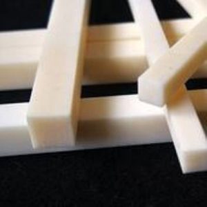
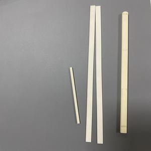
Description
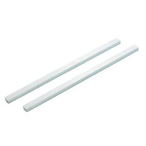
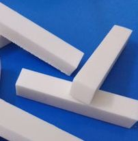
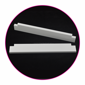
Overview of Ceramic 96 99.6% Alumina Thin Aluminum Oxide Wafer for Semiconductors
Ceramic 96 99.6% Alumina Thin Aluminum Oxide Wafer for Semiconductors are one of the most widely used and versatile technical ceramics, prized for their excellent combination of properties. Composed primarily of aluminum oxide (Al₂O₃), they offer outstanding hardness, wear resistance, and electrical insulation, even at high temperatures. From low-purity grades for general industrial use to high-purity compositions for demanding applications, alumina ceramics provide a cost-effective and reliable solution across a vast range of industries.
Features of Ceramic 96 99.6% Alumina Thin Aluminum Oxide Wafer for Semiconductors
-
High Hardness & Wear Resistance: Excellent resistance to abrasive wear, making it ideal for liners, nozzles, and guides.
-
Superior Electrical Insulation: Maintains high electrical resistivity and dielectric strength, even at elevated temperatures.
-
Excellent Thermal Stability: Withstands high operating temperatures and exhibits good thermal conductivity.
-
High Mechanical Strength: Possesses good compressive strength and stiffness.
-
Chemical Inertness: Resists corrosion from a wide range of acids, alkalis, and other harsh chemicals.
-
Cost-Effectiveness: A highly versatile and economically efficient ceramic material for numerous applications.
Specification of Ceramic 96 99.6% Alumina Thin Aluminum Oxide Wafer for Semiconductors
This wafer is made from ceramic. It makes use of alumina. The alumina material is high. It is 96%. The pureness is also high. It gets to 99.6%. It is slim. This thinness is important. It is developed for semiconductor usages. Semiconductors require dependable parts.
The product gives excellent electrical insulation. Electrical power does not go through easily. It additionally takes care of heat well. It relocates warmth away from delicate parts. This avoids overheating. Chemical stability is an additional vital attribute. It withstands strong acids and bases. This is crucial in chip production. The processes are harsh.
Mechanical stamina is excellent. It does not damage easily under stress. It can hold up against the manufacturing atmosphere. The surface area is extremely smooth. This flatness is crucial. Semiconductor layers are built on top. Any roughness causes defects. Precision is non-negotiable.
It serves as a substrate or service provider. Fragile silicon wafers remain on it. It sustains them throughout handling. The wafer shields the silicon. It manages high temperatures. Heating system actions prevail. It also manages thermal tension. Materials broaden when hot. They agreement when cool. This wafer handles those adjustments well.
Dimensional precision is precise. Resistances are really tight. Also little mistakes destroy chips. Consistency is kept batch after set. Integrity is essential in manufacturing. This ceramic wafer supplies that. It is a reputable component. Semiconductor producers trust it.
Applications of Ceramic 96 99.6% Alumina Thin Aluminum Oxide Wafer for Semiconductors
This ceramic wafer is made from 99.6% pure light weight aluminum oxide. It is a slim, high-purity alumina ceramic. Individuals utilize it a whole lot in the semiconductor market. Its extreme pureness is important. This pureness means fewer pollutants disrupt digital processes. The wafer surface is additionally extremely smooth. This level of smoothness is crucial for accurate semiconductor manufacturing actions. It enables exact photolithography and thin film deposition.
The product handles high temperatures well. It is thermally secure. This stability is essential throughout semiconductor processing. Many steps involve considerable warmth. The wafer will not warp or degrade conveniently. Its high strength includes sturdiness. This stamina protects against damage throughout handling and handling. It is additionally an exceptional electrical insulator. This shielding property is essential. It stops electric disturbance between circuits.
Suppliers rely upon this wafer as a substrate. They build silicon chips on it. It is also utilized as a provider wafer. It supports various other delicate wafers during processing. Its stability makes it appropriate for numerous process chambers. It is utilized in oxidation, diffusion, and annealing heating systems. Its chemical resistance is one more advantage. It endures severe chemicals used in etching and cleansing. This resistance guarantees lengthy service life. The wafer helps achieve high yields in semiconductor production.
Company Profile
Tanki New Materials Co.Ltd. focus on the research and development, production and sales of ceramic products, serving the electronics, ceramics, chemical and other industries. Since its establishment in 2015, the company has been committed to providing customers with the best products and services, and has become a leader in the industry through continuous technological innovation and strict quality management.
Our products includes but not limited to Aerogel, Aluminum Nitride, Aluminum Oxide, Boron Carbide, Boron Nitride, Ceramic Crucible, Ceramic Fiber, Quartz Product, Refractory Material, Silicon Carbide, Silicon Nitride, ect. please feel free to contact us.
Payment Methods
T/T, Western Union, Paypal, Credit Card etc.
Shipment Methods
By air, by sea, by express, as customers request.
5 FAQs of Ceramic 96 99.6% Alumina Thin Aluminum Oxide Wafer for Semiconductors
This ceramic wafer is for semiconductors. It uses high-purity alumina. Alumina is aluminum oxide. The purity is 99.6%. This is very high. High purity means better performance. The wafer is very thin. Thinness is important. It allows for precise use. Alumina has key properties. It insulates electricity well. It handles high heat. It resists chemicals. It is very hard. These properties are vital for semiconductors. They ensure reliability. They ensure stability. The wafer provides a stable base. Components attach to it. Circuits build on it. It must not conduct electricity. Good insulation prevents short circuits. High heat tolerance is crucial. Semiconductors get hot. The wafer must not warp. Chemical resistance protects the wafer. Harsh chemicals are used in manufacturing. The wafer stays intact. Its hardness prevents damage. It withstands handling. This wafer is essential. It supports advanced electronics. It is used in chip making. It is used in sensor production. It is used in various devices. Demand for such components is high. Technology keeps advancing. This alumina wafer meets tough requirements. Its purity guarantees quality. Its thinness enables miniaturization. Manufacturers trust this material. It delivers consistent results. It is a fundamental piece. It supports modern electronics.
REQUEST A QUOTE
RELATED PRODUCTS
96% 99.6% Al2O3 Ceramic Substrate Ultra Thin Aluminum Oxide Alumina Sheet
White Color 95% Aluminum Oxide Alumina Ceramic Bush with Slot
China Factory Industrial Aluminum Oxide Alumina Ceramic Metalized Substrate
Customizable Size Alumina Ceramic Parts Aluminum Oxide Corrosion Resistance Ceramic Shaft for Water Pump
125mm 100mm Grinder Ceramic Zirconium Aluminum Oxide Silicon Carbide Fibre Discs Paper