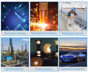
Professional industry ceramic supplier, silicon nitride, silicon carbide, aluminum nitride and any other kinds of ceramics.
1. Introduction
Just 24 hours ago, Wolfspeed announced a major expansion of its silicon carbide wafer production facility in Germany—citing crucible performance as a key bottleneck in scaling output. This news underscores a quiet but pivotal truth in the semiconductor supply chain: the humble silicon carbide crucible is now mission-critical hardware for next-generation electronics.
While most people associate ceramics with dinnerware or tiles, advanced industrial ceramics like silicon carbide crucibles operate in extreme environments where failure isn’t an option. In this article, we’ll dive into one of the most demanding applications for these components: growing ultra-pure silicon carbide single crystals for power semiconductors.
2. Why Silicon Carbide Crucibles? The Physics of Purity
Growing semiconductor-grade SiC crystals requires temperatures above 2,200°C in inert atmospheres. At these extremes, conventional ceramic crucibles—like those made from alumina (Al2O3) or zirconia (ZrO2)—can react with the molten SiC or release impurities that ruin crystal quality.
Silicon carbide crucibles, by contrast, are chemically compatible with the melt. Because they’re made from the same base material as the crystal being grown, they minimize contamination. This self-compatibility is unmatched—even boron carbide vs silicon carbide comparisons show SiC’s superior stability in SiC-rich environments.
- High thermal conductivity prevents hot spots that cause defects
- Exceptional thermal shock resistance allows rapid heating/cooling cycles
- Near-zero reactivity with molten SiC preserves dopant profiles

3. Real-World Application: Physical Vapor Transport (PVT) Furnaces
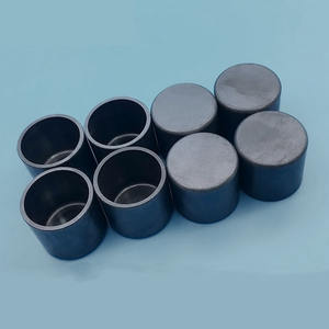
The dominant method for producing SiC wafers is Physical Vapor Transport (PVT). In a PVT furnace, solid SiC powder sublimates at the bottom of a sealed chamber and re-deposits as a single crystal on a seed at the top. The entire process happens inside a silicon carbide crucible.
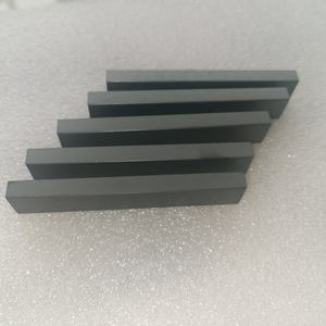
Here, the crucible isn’t just a container—it’s part of the thermal and chemical ecosystem. Engineers often line the crucible with porous silicon carbide ceramic tubes or use rbsic silicon carbide tile blocks to fine-tune vapor flow. Even ancillary parts like silicon carbide burner nozzles and silicon carbide rings must be fabricated from the same high-purity grade to avoid cross-contamination.
4. Material Alternatives and Why They Fall Short
Some manufacturers experiment with silicon nitride crucibles, especially given advances from silicon nitride crucible factories specializing in lab-scale equipment. Silicon nitride ceramic offers good strength and moderate thermal stability, but it decomposes above 1,800°C in vacuum—well below SiC growth temperatures.
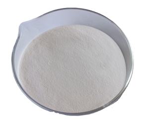
Similarly, zirconia crucibles and alumina crucibles introduce oxygen and metal ions that create deep-level traps in the semiconductor lattice. While useful for lower-temp processes, they’re unsuitable for high-performance SiC wafer production. Even high purity silicon nitride powder market innovations haven’t closed this gap yet.
5. Beyond the Crucible: Integrated SiC Components in Crystal Growth Systems
Modern PVT systems rely on a full suite of silicon carbide-based parts:
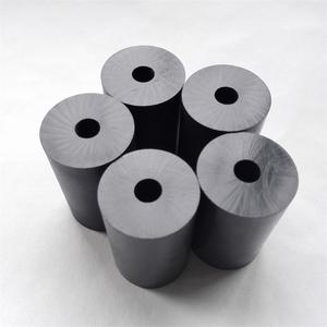
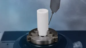
- Silicon carbide ceramic columns support internal fixtures without warping
- Silicon carbide thermocouple protection tubes ensure accurate temperature readings
- Silicon carbide mullite tubes act as diffusion barriers in multi-zone furnaces
These components work together to maintain the ultra-clean, thermally uniform environment needed for defect-free crystal growth. Any weak link—like a standard alumina tube or zirconia rod—can compromise yield.
6. Future Outlook: Scaling Production Without Sacrificing Quality
As demand surges for EV inverters and 5G RF chips, manufacturers are pushing crucible lifetimes and reuse cycles. Recent R&D focuses on recrystallized silicon carbide (R-SiC) and reaction-bonded silicon carbide (RBSC) variants that offer better machinability and longer service life.
Interestingly, some labs are testing hybrid designs—like custom silicon nitride heat shields paired with silicon carbide crucibles—to optimize thermal gradients. But the core containment vessel remains firmly in the silicon carbide domain.
7. Conclusion
From enabling faster-charging EVs to more efficient data centers, the silicon carbide crucible is a silent enabler of the energy transition. Its niche application in semiconductor crystal growth may not make headlines, but without it, the entire wide-bandgap revolution would stall. As Wolfspeed’s expansion shows, mastering this small ceramic component is now a strategic imperative for global tech leadership.
Our Website founded on October 17, 2012, is a high-tech enterprise committed to the research and development, production, processing, sales and technical services of ceramic relative materials such as Silicon. Our products includes but not limited to Boron Carbide Ceramic Products, Boron Nitride Ceramic Products, Silicon Carbide Ceramic Products, Silicon Nitride Ceramic Products, Zirconium Dioxide Ceramic Products, etc. If you are interested, please feel free to contact us.
RELATED POSTS
Silicon Carbide Crucibles: The High-Performance Workhorse of Advanced Ceramics
5 Key Comparisons That Define the Performance of Silicon Carbide Crucibles in Modern Industry

How to Properly Use and Maintain a Silicon Carbide Crucible: A Step-by-Step Guide
How to Properly Use and Maintain a Silicon Carbide Crucible: A Step-by-Step Guide
7 Essential Facts About Silicon Carbide Crucibles and Their Industrial & Kitchen Uses