Professional industry ceramic supplier, silicon nitride, silicon carbide, aluminum nitride and any other kinds of ceramics.
1. Introduction
When you think of cutting-edge tech—from smartphones to electric vehicles—the spotlight often lands on software or circuit design. But behind every microchip is an unsung hero: ultra-pure silicon crystals grown under precisely controlled conditions. And at the heart of this process? The humble yet extraordinary silicon carbide crucible. Far from ordinary labware, these crucibles are engineered components that endure temperatures above 1,500°C while resisting chemical attack from molten silicon—a feat few materials can match.
2. Why Silicon Carbide Crucibles Dominate High-Purity Crystal Growth
In the production of monocrystalline silicon—used for semiconductors and photovoltaics—contamination is the enemy. Even trace impurities from the crucible can ruin an entire ingot. Traditional options like alumina (Al2O3) or zirconia (ZrO2) crucibles may crack under thermal shock or leach oxygen into the melt. Enter silicon carbide (SiC): a material prized for its exceptional thermal conductivity, low thermal expansion, and remarkable chemical inertness at high temperatures.
Silicon carbide crucibles maintain structural integrity during repeated heating and cooling cycles, crucial for processes like the Czochralski (CZ) method. Their ability to withstand molten silicon without significant reaction ensures higher yields and purer crystals—directly impacting chip performance and solar cell efficiency.
3. Silicon Carbide vs. Alternatives: Boron Carbide and Silicon Nitride
While boron carbide (B4C) shares some hardness and thermal properties with SiC, it’s far more expensive and less stable in oxidizing atmospheres—making it impractical for most crystal growth setups. The comparison ‘boron carbide vs silicon carbide’ often ends in favor of SiC for cost, manufacturability, and oxidation resistance.
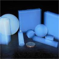
Silicon nitride (Si3N4), another advanced ceramic, offers excellent thermal shock resistance and is used in specialized applications like silicon nitride crucible factories producing lab-scale equipment. However, silicon nitride crucibles are generally not suited for large-scale molten silicon handling due to potential nitrogen contamination and lower thermal conductivity compared to SiC. Components like silicon nitride rings or custom silicon nitride heat shields serve well in support roles, but the crucible itself remains firmly in silicon carbide territory.
4. Advanced Forms: RBSiC and Custom Engineering for Demanding Environments
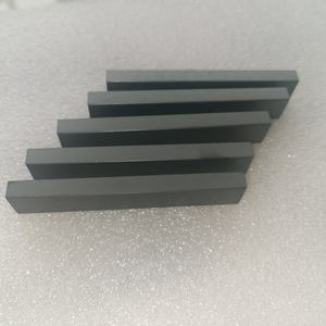
Not all silicon carbide crucibles are created equal. Reaction-bonded silicon carbide (RBSiC)—often seen in forms like rbsic silicon carbide tile blocks or silicon carbide ceramic columns—offers near-net-shape precision, high density, and minimal porosity. This makes RBSiC ideal for crucibles used in directional solidification or float-zone refining, where dimensional stability and purity are non-negotiable.
Manufacturers also produce tailored geometries: thick-walled silicon carbide crucibles with reinforced rims, integrated silicon carbide rings for alignment, or even crucibles paired with silicon carbide thermocouple protection tubes for real-time monitoring. These aren’t off-the-shelf items—they’re mission-critical components designed through advanced ceramics manufacturing.
5. Beyond the Crucible: Supporting Infrastructure in Silicon Carbide
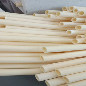
The ecosystem around crystal growth relies heavily on other silicon carbide components. Furnace linings often use silicon carbide brick or silicon carbide ceramic tiles for insulation and durability. Gas delivery systems might incorporate silicon carbide burner nozzles resistant to erosion. Even auxiliary parts like silicon carbide ceramic tubes for high-temperature gas flow or silicon carbide porous ceramic tubes for filtration play supporting roles.
Interestingly, while consumer products like silicon carbide ceramic baking dishes or silicon carbide dinner ceramic plates leverage SiC’s thermal properties for cookware, their composition and purity standards are worlds apart from industrial-grade crucibles. The latter demands ultra-high-purity raw materials and controlled sintering—far beyond what’s needed for a casserole dish.
6. The Future: Purity, Efficiency, and Sustainability
As demand for wider, longer silicon ingots grows—driven by larger wafers for advanced chips and bigger solar panels—the stress on crucibles intensifies. Innovations in silicon carbide processing, such as improved binder systems and densification techniques, aim to extend crucible life and reduce particulate shedding. Some researchers are even exploring hybrid designs combining silicon carbide with thin coatings of pyrolytic boron nitride (PBN) to further minimize interaction with the melt.
Meanwhile, recycling spent crucibles and reclaiming high-purity silicon carbide powder is gaining traction, aligning with sustainability goals in semiconductor manufacturing. The high purity silicon nitride powder market may be booming, but for bulk molten silicon containment, silicon carbide remains unmatched.
7. Conclusion
In the quiet, superheated chambers of crystal pullers worldwide, silicon carbide crucibles perform a vital, invisible service. They bridge materials science and digital innovation, enabling the pure silicon that powers our modern world. While flashy consumer ceramics grab headlines, it’s in these niche industrial applications—where performance trumps aesthetics—that silicon carbide truly proves its worth as an advanced ceramic cornerstone.
Our Website founded on October 17, 2012, is a high-tech enterprise committed to the research and development, production, processing, sales and technical services of ceramic relative materials such as Silicon. Our products includes but not limited to Boron Carbide Ceramic Products, Boron Nitride Ceramic Products, Silicon Carbide Ceramic Products, Silicon Nitride Ceramic Products, Zirconium Dioxide Ceramic Products, etc. If you are interested, please feel free to contact us.
RELATED POSTS
5 Niche Applications of Silicon Carbide Crucibles Beyond Traditional Metallurgy
Silicon Carbide Crucibles: The Backbone of High-Temperature Industrial and Laboratory Applications
How to Properly Use and Maintain a Silicon Carbide Crucible: A Step-by-Step Guide
7 Essential Facts About Silicon Carbide Crucibles and Their Industrial & Kitchen Uses
How to Properly Use and Maintain a Silicon Carbide Crucible to Avoid Common Failures?