Professional industry ceramic supplier, silicon nitride, silicon carbide, aluminum nitride and any other kinds of ceramics.
1. Introduction
Just 24 hours ago, semiconductor giant Wolfspeed announced a $5 billion expansion of its silicon carbide wafer manufacturing facility in Germany—part of a global race to scale up SiC production for electric vehicles and next-gen power electronics. At the heart of this high-stakes manufacturing process lies a surprisingly unsung hero: the silicon carbide crucible.
While most people associate crucibles with ancient metallurgy or chemistry labs, modern silicon carbide crucibles are engineered marvels enabling the production of ultra-pure semiconductor crystals. Their unique combination of thermal stability, chemical inertness, and mechanical strength makes them indispensable in one of today’s most demanding industrial niches.
2. Why Silicon Carbide Crucibles? The Demands of Crystal Growth
2.1. The Physical Vapor Transport (PVT) Process
Producing single-crystal silicon carbide wafers relies heavily on the Physical Vapor Transport (PVT) method. In this process, high-purity SiC powder is heated to over 2,200°C in a vacuum or inert atmosphere. The vapor sublimates and then re-crystallizes on a seed crystal, slowly forming a boule that’s later sliced into wafers.
This extreme environment demands a crucible that won’t crack, react, or contaminate the melt. Standard alumina (Al2O3) or zirconia crucibles fail here—they either degrade or introduce impurities that ruin semiconductor performance. Enter the silicon carbide crucible.
2.2. Material Superiority in Harsh Conditions
Silicon carbide crucibles excel because they’re made from the same base material as the product being grown. This minimizes chemical interaction and thermal mismatch. They offer:
- Exceptional thermal conductivity (up to 120 W/m·K), enabling uniform heating
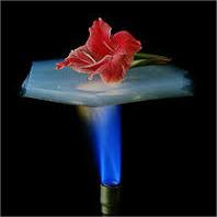
- High resistance to thermal shock, critical during rapid heating/cooling cycles
- Minimal outgassing at ultra-high temperatures
- Excellent mechanical strength even above 1,600°C
These properties ensure consistent crystal quality—essential for high-yield semiconductor manufacturing.
3. Silicon Carbide vs. Alternatives: A Crucible Showdown
3.1. Boron Carbide vs Silicon Carbide
Boron carbide (B4C) is harder and lighter, often used in armor and abrasives. But in crucible applications, it’s less stable above 2,000°C and can release boron vapor that contaminates SiC crystals. For semiconductor-grade purity, silicon carbide wins decisively.
3.2. Silicon Nitride: A Contender with Limitations
Silicon nitride (Si3N4) crucibles—produced by specialized silicon nitride crucible factories—offer great thermal shock resistance and are used in some lab-scale crystal growth. However, they tend to decompose in the reducing atmospheres typical of PVT processes. Plus, high purity silicon nitride powder market constraints make them cost-prohibitive for mass production.
While custom silicon nitride heat shields and silicon nitride rings serve well in furnace insulation, they don’t replace silicon carbide crucibles in the core reaction zone.
4. Beyond the Crucible: Supporting Advanced Ceramic Components
The same advanced ceramic ecosystem that produces silicon carbide crucibles also yields critical auxiliary parts. These include:
- Silicon carbide ceramic tubes for thermocouple protection in high-temp zones
- RBSiC silicon carbide tile blocks for furnace linings
- Silicon carbide burner nozzles and silicon carbide bricks for structural integrity
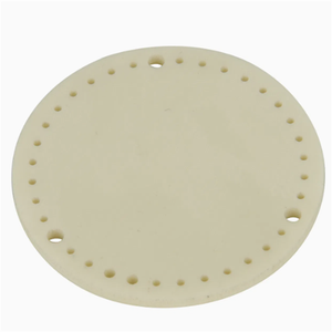
- Silicon carbide ceramic columns and rings for precise gas flow control
Even silicon carbide discs and grinding tools—like silicon carbide diamond grinding discs for pottery—are repurposed in wafer slicing and polishing stages, showing how this material permeates the entire production chain.
5. The Bigger Picture: From Crucibles to Consumer Tech
It’s easy to overlook how a simple crucible enables the EV revolution. Each silicon carbide wafer grown in a silicon carbide crucible powers inverters that boost EV range by 5–10%. With automakers like Tesla and BMW rapidly adopting SiC-based power modules, demand for high-performance crucibles is surging.
Interestingly, the same material science behind these crucibles also enables consumer products—like silicon carbide ceramic baking dishes or silicon carbide ceramic dinner plates—but those use lower-purity, sintered forms. Semiconductor applications require near-theoretical density and parts-per-billion purity levels.
6. Conclusion
The silicon carbide crucible may look like a simple container, but it’s a linchpin in the advanced ceramics supply chain for semiconductors. As the world races to electrify transportation and build 5G infrastructure, this niche application will only grow more critical. Far from being obsolete labware, today’s silicon carbide crucible is a high-tech enabler—quietly shaping the future, one crystal at a time.
Our Website founded on October 17, 2012, is a high-tech enterprise committed to the research and development, production, processing, sales and technical services of ceramic relative materials such as Silicon. Our products includes but not limited to Boron Carbide Ceramic Products, Boron Nitride Ceramic Products, Silicon Carbide Ceramic Products, Silicon Nitride Ceramic Products, Zirconium Dioxide Ceramic Products, etc. If you are interested, please feel free to contact us.
RELATED POSTS
What Makes Silicon Carbide Crucibles Essential in Modern High-Temperature Applications?
5 Common Problems with Silicon Carbide Crucibles—and How to Fix Them
Why Are Silicon Carbide Crucibles Essential in Advanced Semiconductor Crystal Growth?

How Do You Prevent Cracking and Extend the Life of a Silicon Carbide Crucible?
Why Is Silicon Carbide Crucible Essential in High-Temperature Crystal Growth?