Professional industry ceramic supplier, silicon nitride, silicon carbide, aluminum nitride and any other kinds of ceramics.
PRODUCT PARAMETERS
Description
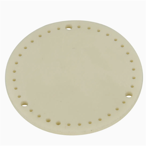
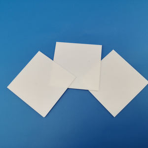
Overview of 6inch 8inch 6″ 8″ Polished or Lapped Sides Aln Aluminum Nitride Wafer for Semiconductors Manufacturing
6inch 8inch 6″ 8″ Polished or Lapped Sides Aln Aluminum Nitride Wafer for Semiconductors Manufacturing is an advanced technical ceramic renowned for its exceptional thermal conductivity and reliable electrical insulation. It is a key material in high-power electronics, LED lighting, and semiconductor processing, effectively managing heat in demanding applications where performance and reliability are critical.
Features of 6inch 8inch 6″ 8″ Polished or Lapped Sides Aln Aluminum Nitride Wafer for Semiconductors Manufacturing
- High Thermal Conductivity: Offers excellent heat dissipation, comparable to beryllia (BeO).
- Electrical Insulation: Maintains high electrical resistivity even at elevated temperatures.
- Low Thermal Expansion: Matches the coefficient of thermal expansion of silicon, ideal for semiconductor substrates.
- Excellent Mechanical Strength: Possesses good mechanical properties for structural integrity.
- High-Temperature Stability: Performs reliably in harsh environments and at high temperatures.
- Non-Toxic: A safe alternative to beryllium oxide (BeO) ceramics.
Specification of 6inch 8inch 6″ 8″ Polished or Lapped Sides Aln Aluminum Nitride Wafer for Semiconductors Manufacturing
These AlN wafers are essential foundation for sophisticated electronics. We supply 6-inch and 8-inch Aluminum Nitride wafers. They come polished or washed on the sides. This makes them ready for semiconductor manufacturing actions.
The wafers are made from high-purity Light weight aluminum Nitride product. Aluminum Nitride provides exceptional thermal conductivity. It deals with warm effectively. This is essential for high-power devices and demanding applications. It likewise offers solid electrical insulation buildings. These homes make it reputable for electronic circuits.
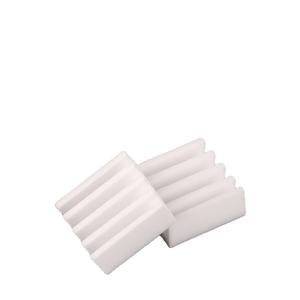
You get an option between polished surfaces or lapped coatings. Polishing produces a very smooth leading surface area. This smoothness is needed for precise micro-circuit construction. Lapped surface areas provide a regulated flatness. Both alternatives meet strict semiconductor industry requirements.
We manage the wafer thickness extremely carefully. Flatness is maintained across the entire wafer surface. This stops warping throughout high-temperature handling. Side high quality is likewise taken care of. Clean, distinct sides reduce bit contamination dangers.
The wafers have reduced surface roughness. Surface area roughness influences movie bond in the future. We additionally monitor surface area problems carefully. Less problems imply higher production returns for our consumers. Crystal alignment is one more essential criterion. It impacts the electrical buildings of the last device.
Material pureness is important. High purity makes certain constant performance. Trace steels and other impurities are minimized. This avoids undesirable electrical leak. Our quality control consists of visual inspection. We likewise make use of assessment tools to inspect dimensions and surface area top quality.
These AlN wafers support the production of LEDs. They are utilized in power gadgets as well. High-frequency RF components additionally rely on them. Semiconductor suppliers need trustworthy substratums. Our Aluminum Nitride wafers supply that structure. They make it possible for the development of effective, lasting electronic items.
Applications of 6inch 8inch 6″ 8″ Polished or Lapped Sides Aln Aluminum Nitride Wafer for Semiconductors Manufacturing
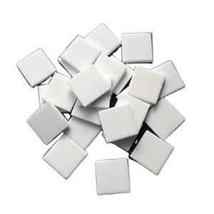
These wafers are made from light weight aluminum nitride (AlN). They are available in sizes of 6 inches and 8 inches. The sides are polished or lapped. This makes them extremely smooth and level. This is important for making sophisticated digital gadgets. Semiconductor producers need such precision.
Light weight aluminum nitride has exceptional properties. It deals with high warm very well. This makes these wivvers excellent for power electronics. Instruments like transistors and diodes create significant heat. The AlN wafer helps pull that warm away. This protects against the gadget from overheating and failing. Reliability boosts substantially.
These wafers additionally work well for high-frequency applications. Think of gadgets used in cordless interaction and radar systems. Light weight aluminum nitride allows electric signals to travel fast with low loss. This is important for 5G innovation and satellite communications. Performance relies on this product.
One more crucial location is optoelectronics. This includes tools dealing with light, like LEDs and sensors. Aluminum nitride is transparent to infrared light. It additionally works as a secure base for expanding special crystal layers. These layers are important for high-performance light-emitting tools. The wafer provides the structure.
The larger 8-inch dimension supplies advantages. More chips can be made on a solitary wafer. This improves production efficiency and reduces costs. Both 6-inch and 8-inch dimensions are in need. The option depends on the details production process and tool kind.
Polishing or splashing the sides guarantees top quality. It removes surface issues. This results in much better bonding with other products during chip fabrication. Tool performance and return rates gain from this smoothness. Producers depend on this top quality.

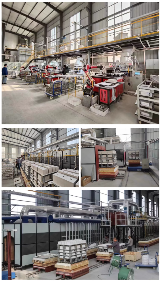
Company Profile
Tanki New Materials Co.Ltd. focus on the research and development, production and sales of ceramic products, serving the electronics, ceramics, chemical and other industries. Since its establishment in 2015, the company has been committed to providing customers with the best products and services, and has become a leader in the industry through continuous technological innovation and strict quality management.
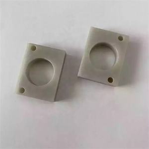
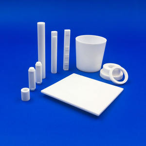
Our products includes but not limited to Aerogel, Aluminum Nitride, Aluminum Oxide, Boron Carbide, Boron Nitride, Ceramic Crucible, Ceramic Fiber, Quartz Product, Refractory Material, Silicon Carbide, Silicon Nitride, ect. please feel free to contact us.
Payment Methods
T/T, Western Union, Paypal, Credit Card etc.
Shipment Methods
By air, by sea, by express, as customers request.
5 FAQs of 6inch 8inch 6″ 8″ Polished or Lapped Sides Aln Aluminum Nitride Wafer for Semiconductors Manufacturing
Here are 5 common questions about our 6-inch and 8-inch Aluminum Nitride (AlN) wafers. These wafers have polished or lapped sides. They are used in making semiconductors.
What are Aluminum Nitride wafers?
Aluminum Nitride wafers are thin discs. They are made from Aluminum Nitride ceramic material. This material is very hard. It handles high heat and electricity well. The wafers provide a base for building electronic parts.
What sizes are available?
We offer two main sizes. These are 6-inch (150mm) and 8-inch (200mm) wafers. Both sizes are common in chip factories. The 8-inch size allows more chips per wafer. This saves money on big production runs.
What does polished or lapped sides mean?
Polished sides are very smooth. They have a mirror-like finish. Lapped sides are smoother than rough cut. But they are not as shiny as polished. Polished is better for fine, detailed chip work. Lapped is often good enough and costs less.
Why use Aluminum Nitride?
Aluminum Nitride has special benefits. It moves heat away fast. This keeps chips cooler. It also insulates electricity well. It does not expand much with heat. These features make it perfect for powerful electronics and LEDs.
Where are these wafers used?
These wafers go into many high-tech devices. They are key for radio frequency chips. They help make power amplifiers. They are used in LED lighting systems. They support advanced sensors. They are also found in some laser products.
REQUEST A QUOTE
RELATED PRODUCTS
Factory Customized Square Wear-Resistant High Thermal Conductivity Low Dielectric Loss Aluminum Nitride Ceramic Substrate High Temperature Resistant
Aluminum Nitride Crucible for Crystal Growth Processes
Premium 99.99% Aluminum Nitride Ceramics, Moulding Plus Machining by Gravel
Custom Wear-Resistant Thermal Conductive Aluminum Nitride Ceramic Disc Size Thickness Dimensions Customized According to Drawings China Factory Whole
Composite Boron Nitride+Aluminum Nitride Textile-Traversing Wire Guide