Professional industry ceramic supplier, silicon nitride, silicon carbide, aluminum nitride and any other kinds of ceramics.
PRODUCT PARAMETERS
Description
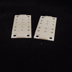
Overview of Laser Scribing High Thermal Conductivity Aln Ceramic Aluminum Nitride Substrate
Laser Scribing High Thermal Conductivity Aln Ceramic Aluminum Nitride Substrate is an advanced technical ceramic renowned for its exceptional thermal conductivity and reliable electrical insulation. It is a key material in high-power electronics, LED lighting, and semiconductor processing, effectively managing heat in demanding applications where performance and reliability are critical.
Features of Laser Scribing High Thermal Conductivity Aln Ceramic Aluminum Nitride Substrate
- High Thermal Conductivity: Offers excellent heat dissipation, comparable to beryllia (BeO).
- Electrical Insulation: Maintains high electrical resistivity even at elevated temperatures.
- Low Thermal Expansion: Matches the coefficient of thermal expansion of silicon, ideal for semiconductor substrates.
- Excellent Mechanical Strength: Possesses good mechanical properties for structural integrity.
- High-Temperature Stability: Performs reliably in harsh environments and at high temperatures.
- Non-Toxic: A safe alternative to beryllium oxide (BeO) ceramics.
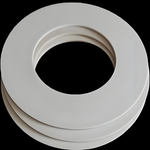
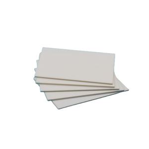
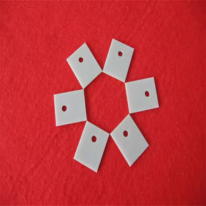
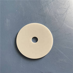
Specification of Laser Scribing High Thermal Conductivity Aln Ceramic Aluminum Nitride Substrate
Laser scribed Aluminum Nitride (AlN) ceramic substrates offer exceptional thermal performance. This material handles high heat extremely well. AlN ceramic has a thermal conductivity much greater than standard alumina ceramics. Heat moves through it very efficiently. This is vital for modern electronics. Powerful devices generate significant heat. Good heat management prevents failure. AlN substrates move heat away from sensitive components fast. This keeps everything running cooler and more reliably.
Engineers choose AlN for demanding applications. Power electronics modules need this thermal capability. High-brightness LED lighting systems benefit greatly. Advanced semiconductor packages rely on it. RF and microwave components also use AlN substrates. The material handles electrical insulation effectively too. Its electrical properties are excellent. It resists electrical current flow well. This prevents short circuits. AlN also matches silicon in how it expands and contracts with heat changes. This reduces stress on attached components. It improves the long-term reliability of the whole assembly.
Precise laser scribing creates clean separation lines on the AlN substrate surface. This allows controlled breakage into individual chips later in production. Laser processing is highly accurate. It minimizes material waste. It ensures clean edges on the final parts. This precision is essential for complex circuits and tight component spacing. The process is suitable for thin, fragile wafers. It maintains the substrate’s inherent strength and thermal properties right up to the edge. This consistency is crucial for performance. Manufacturers value the repeatability laser scribing provides. It supports high-volume production.
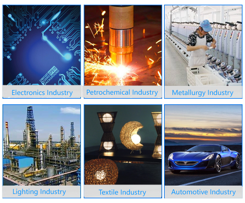
Applications of Laser Scribing High Thermal Conductivity Aln Ceramic Aluminum Nitride Substrate
Laser scribing cuts precise patterns on aluminum nitride ceramic substrates. This material handles heat very well. Electronics need this ability. Laser processing makes clean, narrow grooves in AlN. This is vital for making circuit boards from these ceramics. Traditional cutting methods often crack or chip AlN. Lasers avoid this problem. The heat affected zone near the laser cut is very small. This keeps the material strong around the cut lines.
Manufacturers use laser scribing for AlN substrates in many demanding areas. Power electronics rely on these substrates. Devices like IGBTs and power modules generate intense heat. AlN spreads this heat fast. Laser scribing defines the metal pathways on the substrate. These pathways carry high currents. Clean laser cuts prevent electrical shorts. The process ensures tight tolerances for complex circuit designs.
LED production also uses laser-scribed AlN. High-power LED chips get extremely hot. Aluminum nitride substrates manage this heat effectively. Lasers accurately cut the substrate into many small chips or “dice”. This step happens before separating the individual LEDs. Precise laser scribing prevents damage to the fragile LED structures. It guarantees high yields and consistent performance.
Laser processing offers key advantages for AlN. It is a non-contact method. There is no tool wear. It works fast. It allows for high automation levels. Complex patterns are easy to program and repeat exactly. The process is highly controllable. Operators can adjust laser power, speed, and pulse settings. This optimizes the cut for different AlN thicknesses and specific patterns. This flexibility is crucial for modern electronics manufacturing. It supports miniaturization trends. Devices get smaller but more powerful. Efficient heat removal becomes even more critical. Laser scribed AlN substrates meet this need reliably. They are found in advanced communication systems and automotive electronics too. These fields demand robust thermal management.
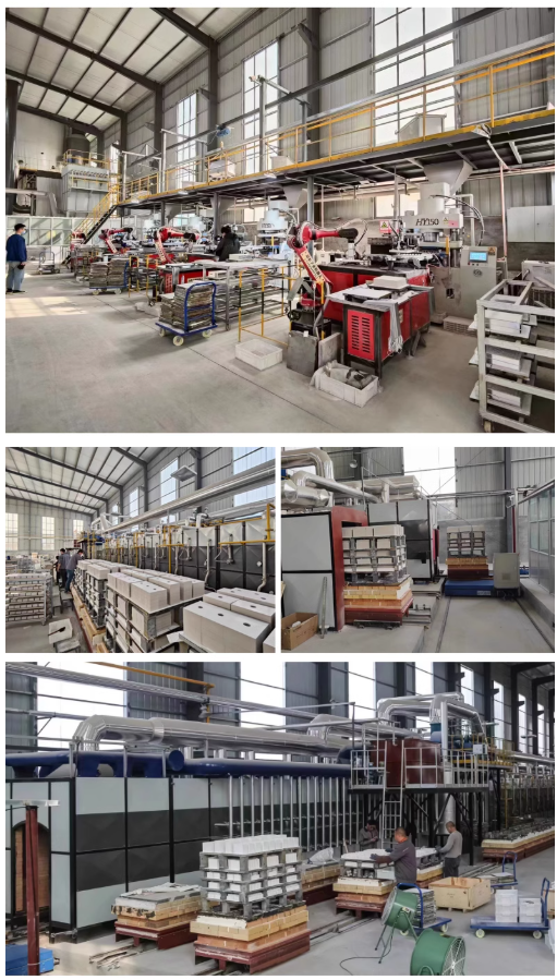
Company Profile
Tanki New Materials Co.Ltd. focus on the research and development, production and sales of ceramic products, serving the electronics, ceramics, chemical and other industries. Since its establishment in 2015, the company has been committed to providing customers with the best products and services, and has become a leader in the industry through continuous technological innovation and strict quality management.
Our products includes but not limited to Aerogel, Aluminum Nitride, Aluminum Oxide, Boron Carbide, Boron Nitride, Ceramic Crucible, Ceramic Fiber, Quartz Product, Refractory Material, Silicon Carbide, Silicon Nitride, ect. please feel free to contact us.
Payment Methods
T/T, Western Union, Paypal, Credit Card etc.
Shipment Methods
By air, by sea, by express, as customers request.
5 FAQs of Laser Scribing High Thermal Conductivity Aln Ceramic Aluminum Nitride Substrate
Customers often ask about laser scribing for high thermal conductivity AlN ceramic substrates. Here are five common questions.
Why use laser scribing on AlN substrates? Lasers offer precise, clean cuts. This is vital for fragile ceramic materials. Traditional mechanical methods can cause chipping or cracking. Lasers minimize this damage. They ensure the substrate edges stay smooth and intact.
What precision can laser scribing achieve? Laser systems deliver very high accuracy. They can create features down to micron levels. This precision is essential for complex circuit patterns. Tight tolerances are needed in advanced electronics packaging. Lasers meet these demands consistently.
Does laser scribing affect thermal performance? Properly controlled laser scribing preserves the substrate’s thermal properties. The heat-affected zone is extremely small. The laser process does not degrade the bulk AlN material. Thermal conductivity remains high across the substrate. Heat dissipation is not compromised.
How deep can the laser scribe lines be? Laser scribing depth is highly controllable. Operators adjust laser power and focus precisely. Scribe depths range from shallow surface marks for break lines. Deeper cuts are possible for specific features. The process adapts to different design requirements.
Can lasers handle very thin AlN substrates? Yes, laser scribing excels with thin, delicate substrates. Mechanical stress is almost non-existent. This prevents warping or breaking during processing. Lasers reliably scribe ultra-thin AlN wafers. This is crucial for miniaturized electronic devices.
REQUEST A QUOTE
RELATED PRODUCTS
99.9% Purity Alumina Ceramic Ball High-Purity Alumina Grinding Media Aluminum Nitride Featuring MGO Alumina Cement Sio2 Welding
Thermal Management Aluminum Nitride Plate Aln Ceramic Substrate for Mosfet
Aluminum Nitride Powder (AlN) Used for High Performance Ceramic Products
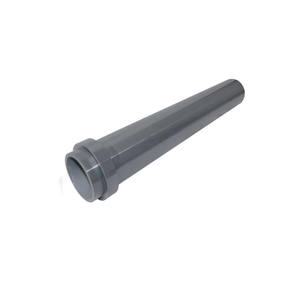
Customized Dielectric Properties Good High Temperature Resistant Insulation Aluminum Nitride Aln Ceramic Rod Roller Cylinder
High Purity Aluminum Nitride Powder CAS 24304-00-5 Good Thermal Conductivity