Professional industry ceramic supplier, silicon nitride, silicon carbide, aluminum nitride and any other kinds of ceramics.
PRODUCT PARAMETERS
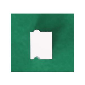
Description
Overview of High Purity Bn Boron Nitride Ceramic Block for Semiconductor Industry
High Purity Bn Boron Nitride Ceramic Block for Semiconductor Industry ceramics are a class of advanced technical ceramics, often referred to as “white graphite.” They are renowned for their unique combination of properties, including high thermal conductivity, excellent electrical insulation, and outstanding thermal shock resistance. Available in various forms such as hot-pressed solids, coatings, and composites, BN ceramics are critical in demanding applications across aerospace, electronics, and metallurgical industries.
Features of High Purity Bn Boron Nitride Ceramic Block for Semiconductor Industry
-
High Thermal Conductivity: Offers excellent heat dissipation, similar to metals, while maintaining electrical insulation.
-
Excellent Thermal Shock Resistance: Withstands extreme and rapid temperature changes without cracking.
-
Superior Electrical Insulation: Maintains high resistivity even at elevated temperatures.
-
Low Dielectric Constant and Loss: Ideal for high-frequency and microwave applications.
-
Good Chemical Inertness: Resists attack from most molten metals, slags, and salts.
-
Non-wetting and Non-reactive: With many molten metals like aluminum and copper.
-
High Temperature Stability: Can be used in inert or vacuum atmospheres up to 3000°C.
-
Machinability: Can be precision-machined into complex shapes using conventional tools, unlike many other advanced ceramics.
Specifications of High Purity Bn Boron Nitride Ceramic Block for Semiconductor Industry
High pureness BN boron nitride ceramic blocks serve critical roles in semiconductor production. This product manages extreme heat well. It moves warmth far from sensitive parts quick. This stops damage during extreme processes. Semiconductor tools demand phenomenal chemical stability. BN ceramic offers solid resistance. It stands up to corrosive gases and liquified metals common in fabs. Electric insulation is one more essential building. BN obstructs accurately isolate electric pathways. This stops hazardous short circuits around wafers.
Product pureness straight impacts chip yields. Also little contaminations trigger issues. Our BN obstructs guarantee purity going beyond 99.99%. We regulate contamination carefully. Trace elements like salt, potassium, iron keep below stringent ppm limitations. Constant purity is non-negotiable for advanced nodes. The ceramic framework provides superb mechanical toughness also. It keeps form under high stress and temperature cycling. This dimensional security makes certain precise tool placement over time.
Machining BN ceramic calls for specialized techniques. We accomplish really tight tolerances and smooth surface finishes. Monotony and similarity fulfill rigorous devices specs. Thermal shock resistance is impressive. BN obstructs sustain quick heating & cooling without splitting. This dependability lessens costly production downtime. Semiconductor engineers select BN for its unique combination of residential or commercial properties. It allows higher process temperatures and cleaner settings vital for next-generation gadgets. Constant efficiency safeguards useful silicon wafers.
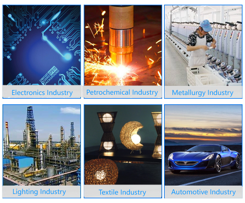
Applications of High Purity Bn Boron Nitride Ceramic Block for Semiconductor Industry
High pureness BN ceramic blocks are important in semiconductor manufacturing. Their severe pureness stops wafer contamination. This product takes care of high temperatures quickly. Semiconductor processes commonly run very hot. BN ceramic stays stable. It does not split or warp. Thermal shock resistance is outstanding. Quick heating and cooling cycles take place usually. BN obstructs manage this without damage.
Electric insulation is another key advantage. BN ceramic does not carry out electrical power. This is crucial around delicate electronic devices. Fixed discharge can spoil semiconductor devices. BN blocks prevent this problem. They keep wafers secure throughout taking care of and refining. Wafer carriers and watercrafts frequently use BN ceramic. It holds silicon wafers securely. The material contacts wafers straight. High purity makes certain no fragments transfer.
Plasma resistance is essential. Lots of semiconductor steps utilize plasma etching. Plasma is extremely responsive. BN ceramic withstands this harsh setting. It does not deteriorate quickly. Refine chamber components benefit from BN linings. These safeguard the chamber wall surfaces. They also keep plasma stability. Regular plasma is needed for consistent etching.
Warm management is vital. BN ceramic spreads warm uniformly. Hot areas cause problems in wafers. BN heater plates provide consistent temperature level. This improves procedure control. Wafer quality depends upon steady temperatures. BN blocks deliver this consistency. They last a long period of time in hard problems. This decreases devices downtime and maintenance costs. Semiconductor makers depend on these residential or commercial properties for high returns.
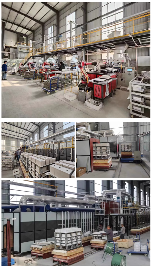
 Company Profile
Tanki New Materials Co.Ltd. focus on the research and development, production and sales of ceramic products, serving the electronics, ceramics, chemical and other industries. Since its establishment in 2015, the company has been committed to providing customers with the best products and services, and has become a leader in the industry through continuous technological innovation and strict quality management.
Our products includes but not limited to Aerogel, Aluminum Nitride, Aluminum Oxide, Boron Carbide, Boron Nitride, Ceramic Crucible, Ceramic Fiber, Quartz Product, Refractory Material, Silicon Carbide, Silicon Nitride, ect. please feel free to contact us.
 Payment Methods
T/T, Western Union, Paypal, Credit Card etc.
Shipment Methods
By air, by sea, by express, as customers request.
5 FAQs of High Purity Bn Boron Nitride Ceramic Block for Semiconductor Industry
What makes this BN ceramic block so pure?
Our blocks use only the cleanest boron nitride powder. We process it carefully. This prevents harmful impurities. Impurities can ruin semiconductor wafers. Our blocks keep wafers safe. We guarantee very low contamination levels. This purity is essential.
How hot can this block get before it fails?
This BN block handles extreme heat well. It works perfectly up to 1800°C in air. It works even hotter in special atmospheres. It won’t crack or melt easily. It handles sudden temperature changes too. This is vital for semiconductor heat processes.
Will this BN block react with chemicals?
No, this BN block is very stable. It resists most acids and bases. It won’t react with molten metals either. This chemical inertness is crucial. It prevents contamination during etching or crystal growth. Your process chemicals stay clean.
Is this BN block a good electrical insulator?
Yes, it’s an excellent insulator. Even at very high temperatures, it blocks electricity. This prevents short circuits. It protects sensitive semiconductor equipment. Good insulation is non-negotiable in fabs.
How do I clean this block safely?
Cleaning is straightforward. Use mild solvents or acids. Avoid harsh abrasives. Gentle cleaning removes residues. It won’t damage the block’s surface. Proper cleaning ensures long life and consistent performance. Follow our simple cleaning guide.
REQUEST A QUOTE
RELATED PRODUCTS
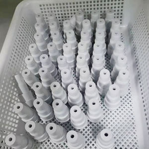
Factory Supply Bn+Zro2+Sic Boron Nitride Precision Part for Ceramic Industry
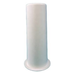
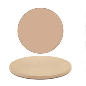
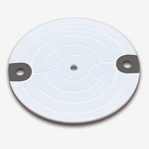
Custom Boron Nitride Ceramic Discs with Excellent Electrical Insulation at High Temperatures
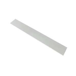
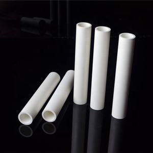
High Thermal Conductivity Tube/Rod/Plate/Heat Sink Boron Nitride /Bn Ceramics
High Thermal Conductive Bn Boron Nitride Ceramics Heat Sink and Plate
Industry Ceramic Furnace Boron Nitride Ceramic Parts